HDI Technology - HiDensity PCB
High-Density Interconnect Printed Circuit Boards (HDI) with Laser-Drilled Microvias
Miniaturisation in electronics is making ever higher demands of printed circuit boards, especially concerning conductor widths, distances and pad density in ball grid array (BGA) areas. The limits of feasibility are quickly reached with mechanical via holes when trying to meet these requirements and the use of lased or mechanically drilled blind holes (microvias) becomes necessary.
Applications:
- network technology
- medical technology
- high frequency technology (impedance behaviour)
Advantages:
- considerable savings in space are realised through significantly smaller drilling diameters
- filled microvias can be placed directly above each other (maximum saving in space)
- the laser technique used to produce the microvias makes it possible to stop exactly at the desired layer. The following dielectric thickness is retained completely
- mechanically drilled blind vias are also possible, as is a combination of lasered and mechanically drilled blind vias
HDI technology is extremely versatile and can be realised practically in every imaginable combination:
- HDI with plugging / copper filling
- HDI with thick copper
- HDI with semiflex
- HDI with metal profiles
- HDI with mixed dielectrics
- HDI with metal inlay
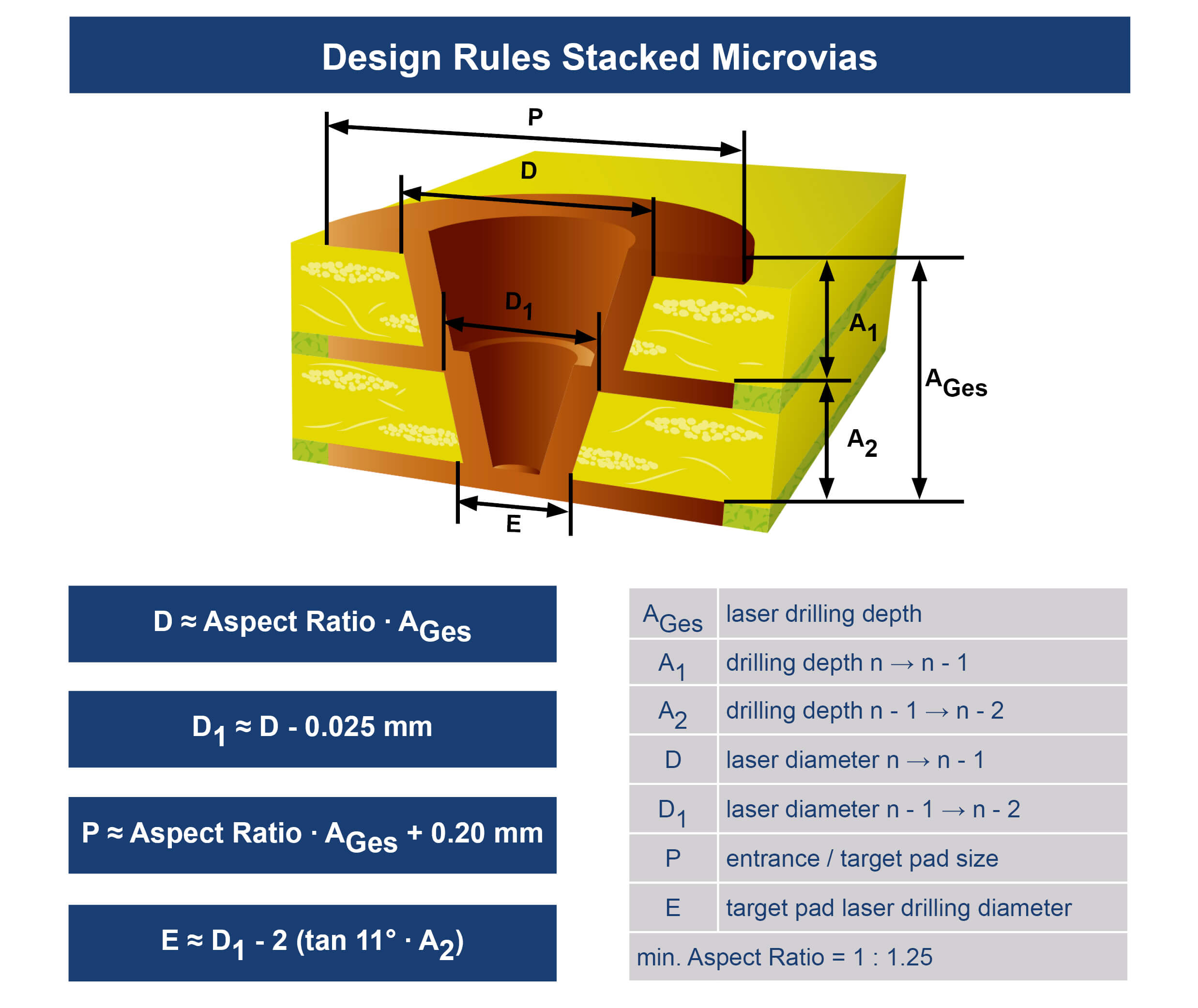
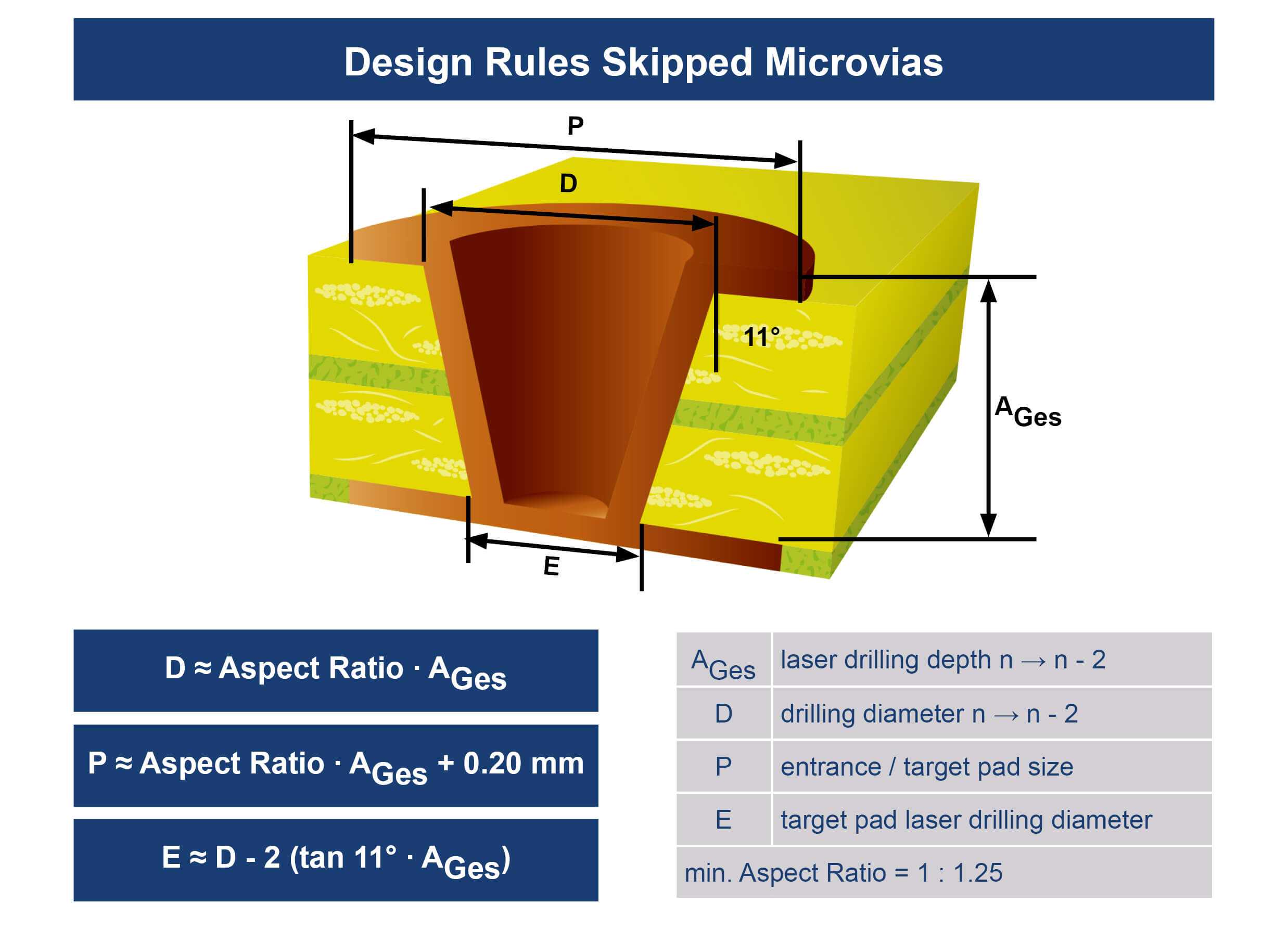
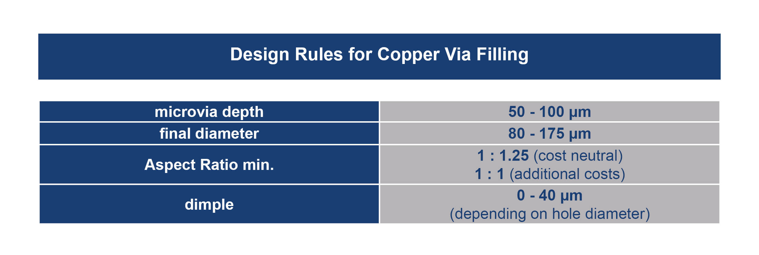
Design Rules:
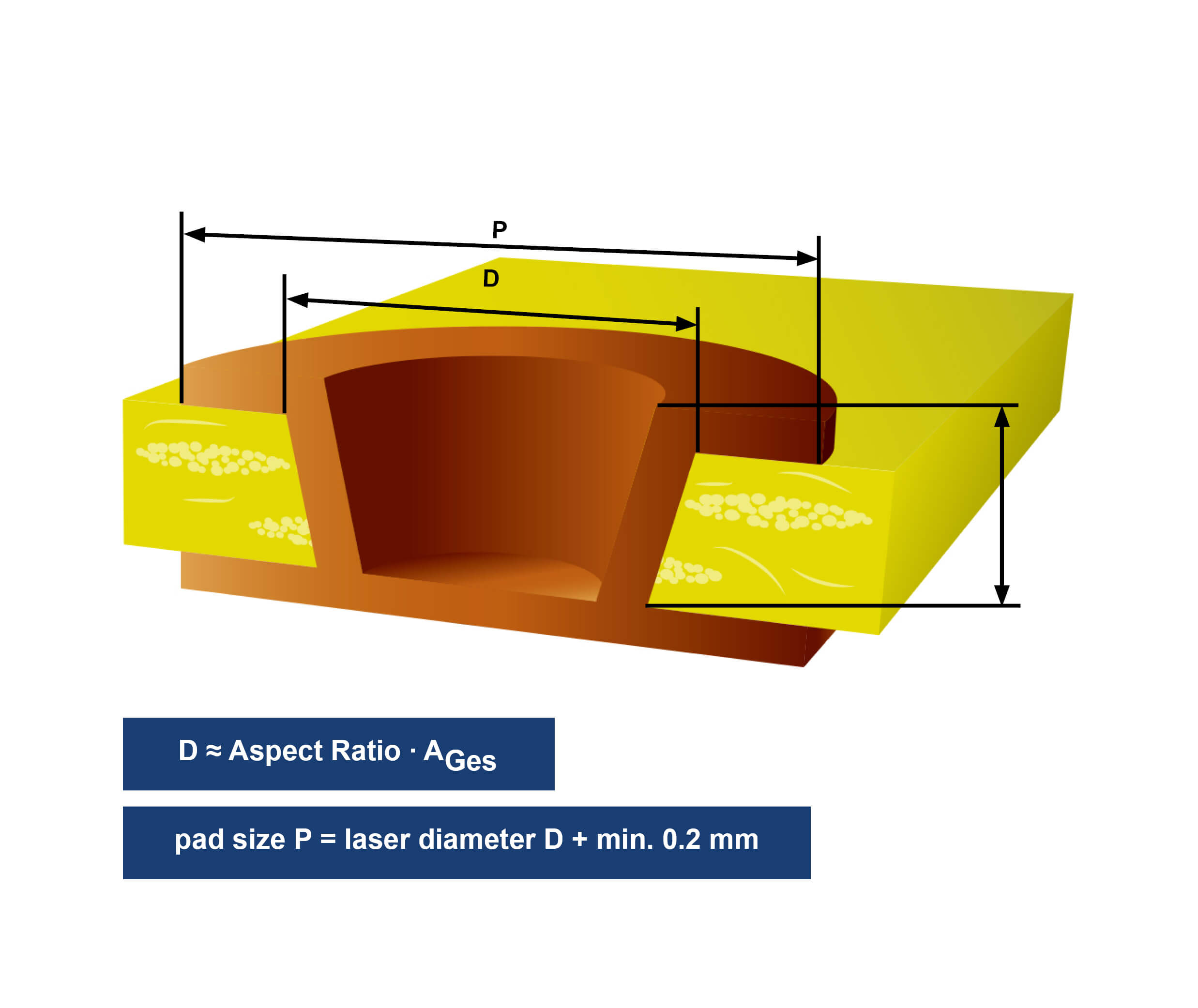
Crucial Quality Parameters:
- value “min. 0.2 mm“ results from tolerance considerations of the laser, dimensional changes and layer distortions
- through hole plating: the decisive factor is the aspect ratio of ≥ 1 :1.25 to ensure a sufficient through hole plating
- minimum thickness of the copper deposit in the microvia: 10 µm
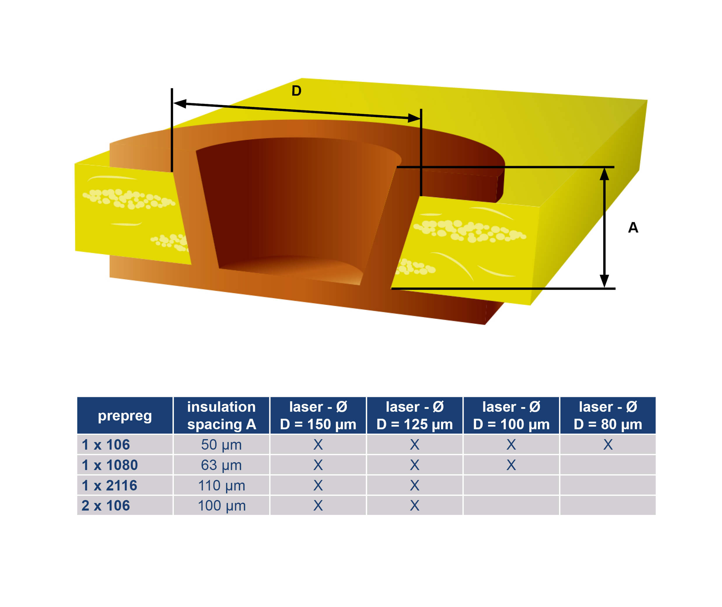
- entrance angle of the laser beam is between 7! and 14! (average 11). Therefore, D is approx. 30% smaller at the target pad. This applies accordingly to the plating surface which is critical for the adhesion pth-copper and base copper.
- if possible, microvias should be designed without clearance in the solder mask
- Note: plated through vias show much earlier cracks in cycling tests, despite 25-30 µm copper in the holes
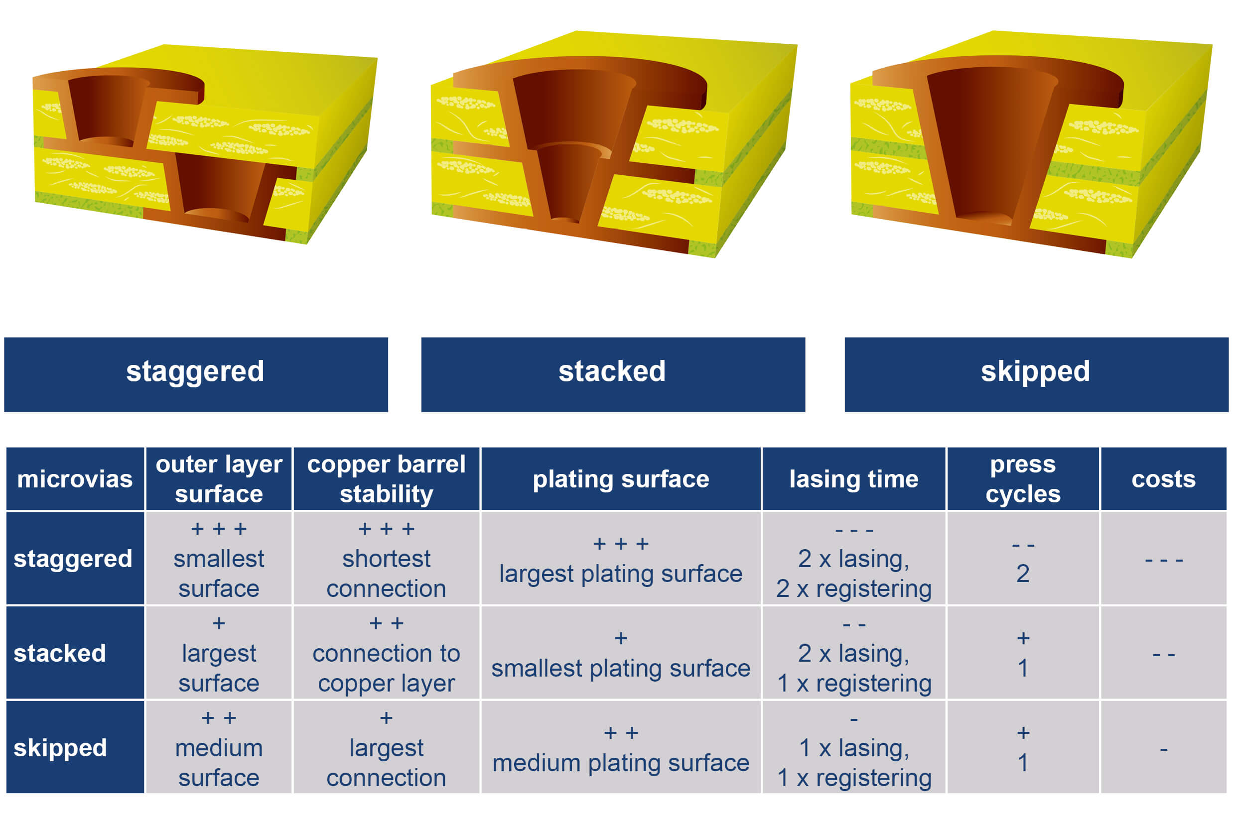
Staggered, Stacked und Skipped Microvias in Comparison:
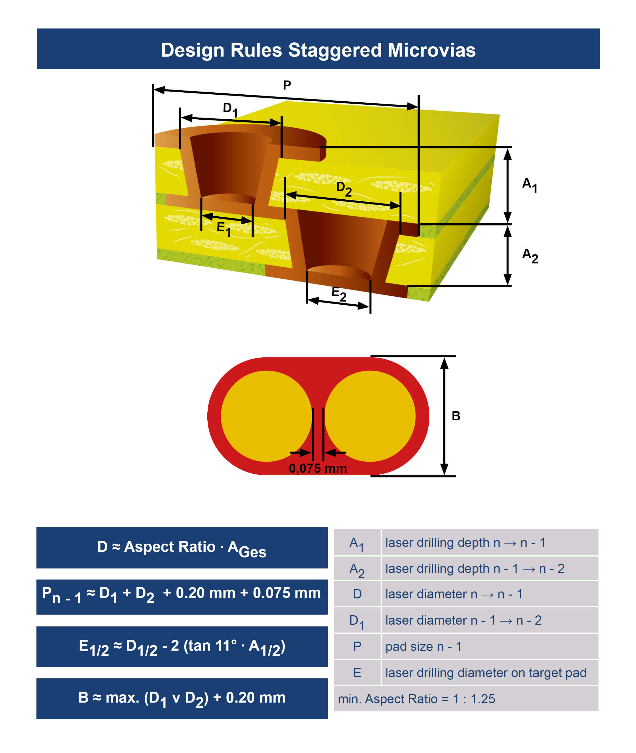
Design Rules for Staggered, Stacked and Skipped Microvias:
Base Materials
Besides “standard“ FR4 materials, filled PTFE materials (such as for example Rogers 3003) may also be lased for high-frequency applications.
We generally recommend that you contact our expert team already before planning a HDI PCB and discuss in detail in order to prevent avoidable problems at an early stage and to develop cost-efficient solutions.
Resin Filling
Filling means closing the holes with resin and grinding the surface, obtaining in this way the planarity of the following layer.
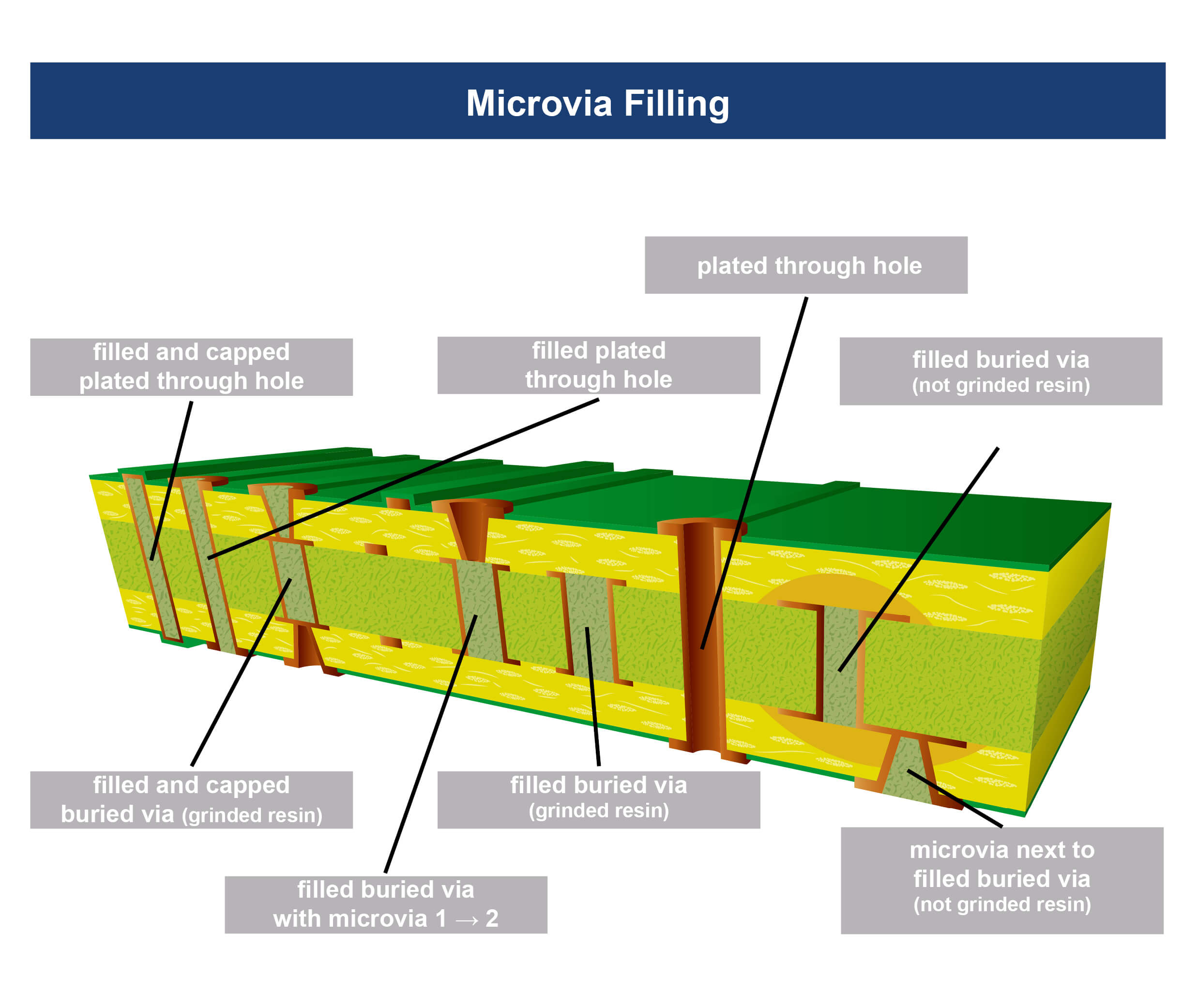
We offer several possible processes for buried vias, which affect the costs. For details please contact our specialists.
Copper Filling
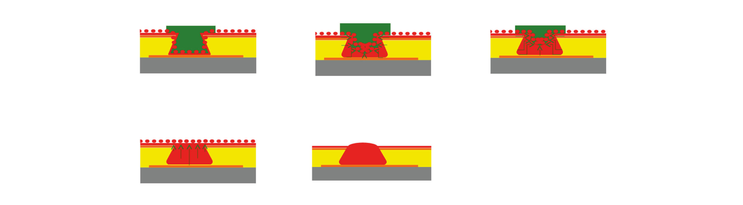
How are blind vias filled with copper?
After the plating through process the hole is filled in a special copper bath. The organic of the copper bath suppresses the deposition on the outer layer and supports the deposition in the blind vias.
Advantages of Copper Filled Vias:
- microvias are nearly completely filled, at the same time only minimal copper deposition on the surface
- established process in the PCB industry
- SBU layouts with copper filled microvias and via-in-pad technology offer 20-40 % more space for routing
- copper filled microvias are more reliable by nature, same CTE as hole wall copper, there is no additional foreign material in the hole
- a much better thermal conductivity compared to organically filled microvias
- excellent signal integrity
Disadvantage:
- higher costs
In order to safely prevent air inclusions (voids) when soldering on blind vias, we recommend to fill the blind vias with copper.
Applications and Advantages of Filled Vias:
- HDI / SBU PCBs which can not be routed otherwise, particularly in BGA areas
- with drilled and filled vias in inner layers there will be no indentations on the layers above, i. e. „fine-line structures“ can be realized there without any problem
- gain of space: with filled and capped buried vias contacting can be realized directly on the pad
- filled via holes / microvias are protected against attacks by fluids and gases
Product Range:
- filling in combination with HDI and SBU
- filling for capped vias
Crucial Quality Factors:
- expansion coefficient of resin and base material
- copper thickness in the drill hole
- adhesion between plugging paste and copper / base material
- requirements made of the paste
- high-TG
- slight to no shrinkage
- chemical stability
- filling is carried out under vacuum in order to prevent air inclusions
Base Materials
Unimicron Germany has generally only approved high-temperature materials (TG ≥ 150°C) for plugging in order to safely prevent copper barrel cracks. All the materials and combinations we use must withstand at least 1,000 temperature cycles -40°C / +140°C.
For filled and buried vias, however a standard base material can be used.
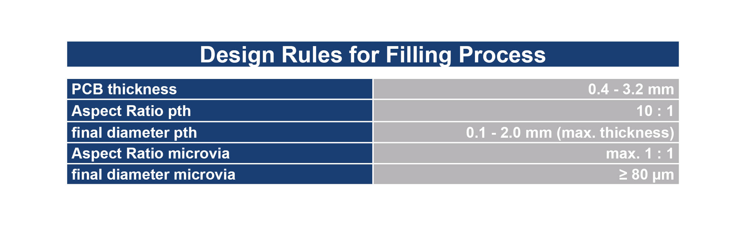
Design Rules for Filling
Knowhow
- high TG materials must always be used
- vacuum-supported plugging process in order to prevent air inclusions as far as possible
- minimum copper thickness in the hole must be 12 μm to safely prevent “blow-holes”
- after planarizing the paste must form a safe bond with the prepregs
We generally recommend that you contact our expert team already before planning a plugged printed circuit board to discuss the PCB in detail in order to prevent avoidable problems at an early stage and to develop cost-efficient solutions.
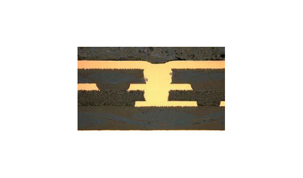
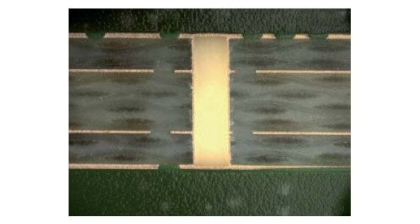
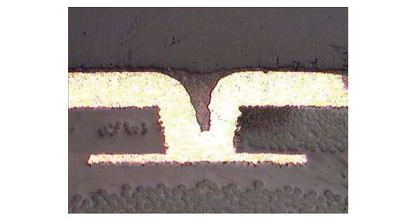
Microsection Examples:
Staggered microvias and filled buried via
Microvias with copper via filling
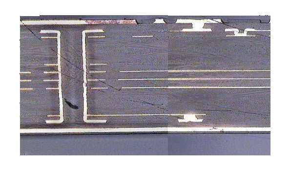
10 layers HDI build up with buried vias
Capped via
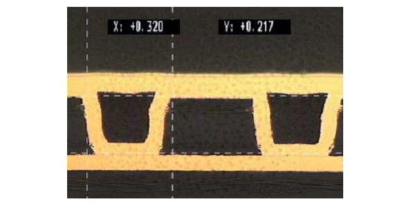
Blind via filled and capped
Filled blind via, not capped
Contact to product management:
product management
+49 (0) 2831 - 3 94-0
info@unimicron.de
Further PCB Technologies:
Thick Copper Technology - HiCu PCB | Thick Copper Profile Technology - HiCu Profile PCB | High Frequency Technology - HiFrequency PCB | Metall Inlay Technology - Metal Inlay PCB | IMS & Heatsink Technology - Metal Plate PCB | Semiflex Technology - Semiflex PCB | Partial Thick Copper Technology - Wirelaid®