Semiflex Technology - Semiflex PCB
Smart Solutions for Optimized Integration
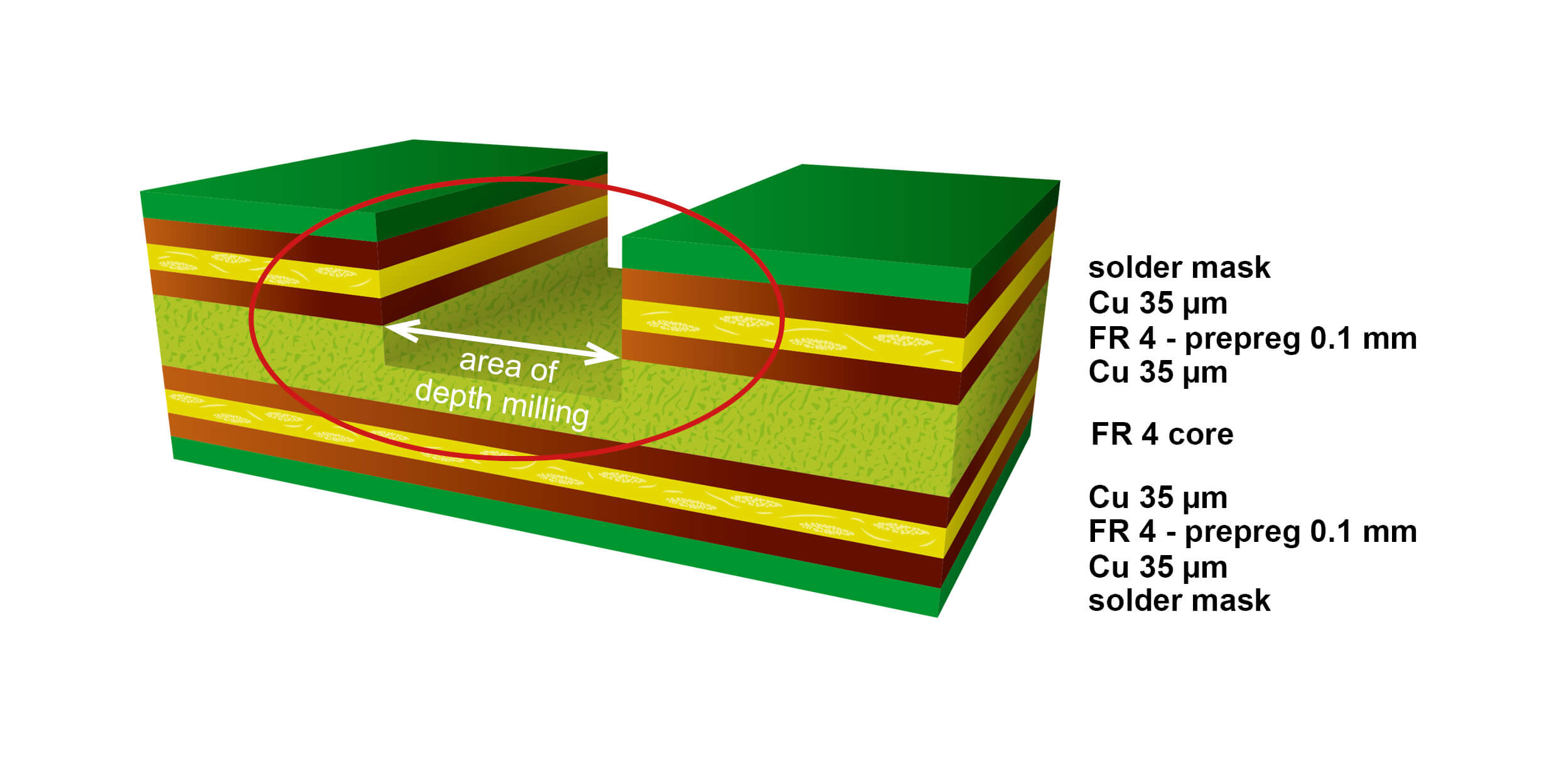
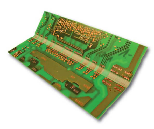
In Semiflex Technology the (semi-) flexible area is produced by defined depth-milling. Semiflex offers an alternative with considerable cost advantages over classic rigid-flex printed circuit boards on a polyimide basis. Thanks to the low moisture absorption of the polyimide-free construction, special thermal pre-treatment for soldering is no longer necessary.
This technology is only suitable for applications where no dynamic stressing of the bending area is required. As a rule, the printed circuit board is bent only once, during mounting of the assembly in the housing. After static fixing of the printed circuit board, further bending cycles may be necessary for service purposes.
Unimicron Germany has been manufacturing and supplying printed circuit boards with semi-flexible areas for all applications for more than 25 years now. Thanks to its high quality and reliability, Semiflex PCB has been approved for use in the automotive industry - for safety electronics too - for more than 20 years.
.
Applications:
- applications with no dynamic stress of the bending area
- automotive
- industrial electronics
- safety electronics
Advantages:
- high reliability
- elimination of components
- space savings
High Reliability and Quality
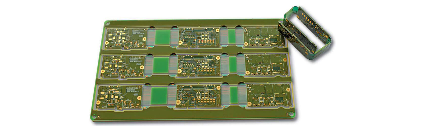
Example: 4 layer multilayer with 2 copper layers in flex-area
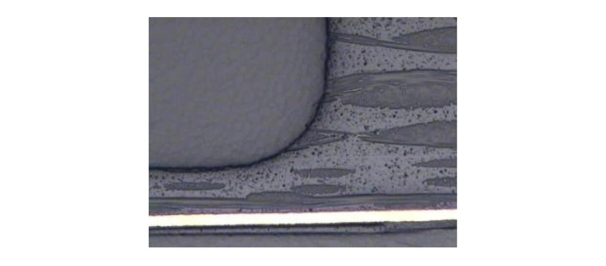
Microsection of a PCB with two copper layers in the flexible area (width 250μm ± 50μm)
Essential Factors for Quality and Reliability and Design Rules:
- The length of the flexible area must correspond to the router diameter, i.e. the flexible area is preferably produced “in one go” (cost-efficient). This has the clear advantage that there are no steps in the flexible area which could later represent a potential weak point for bending. We only carry out multiple millings after explicit agreement with the customer.
-
The routers used for the depth-milling process have a special geometry, safely avoiding “sharp- edge” transitions between the rigid and the flexible area.
-
When milling, the router may not dip into the subsequent semi-flexible area, i.e. a minimum clearance of 0.5 x router diameter + 0.1 mm must be provided for immersion and levelling off of the router outside this area.
-
Copper-free areas must be filled up with non-functional tracks (blind conductors) or copper to increase stability (min. 1 mm overlap in the rigid area).
-
Conductor and blind conductor should be radial to the bending radius.
-
Component holes or SMD pads on the rigid area must have a minimum distance of 1 mm from the flexible area.
-
The minimum conductor widths and spacings (min. 200 μm) depend on the copper thickness, bending radius and bending angle.
-
The outer edges of the flexible areas should have a “tearing protection” (blind conductor) with a minimum width of 1 mm.
-
The layout of the flexible area should as far as possible run in only one direction (x or y), otherwise the flexible mask for the x- and y-directions must be produced in two process steps (increasing the costs!)
Construction Note Bending:
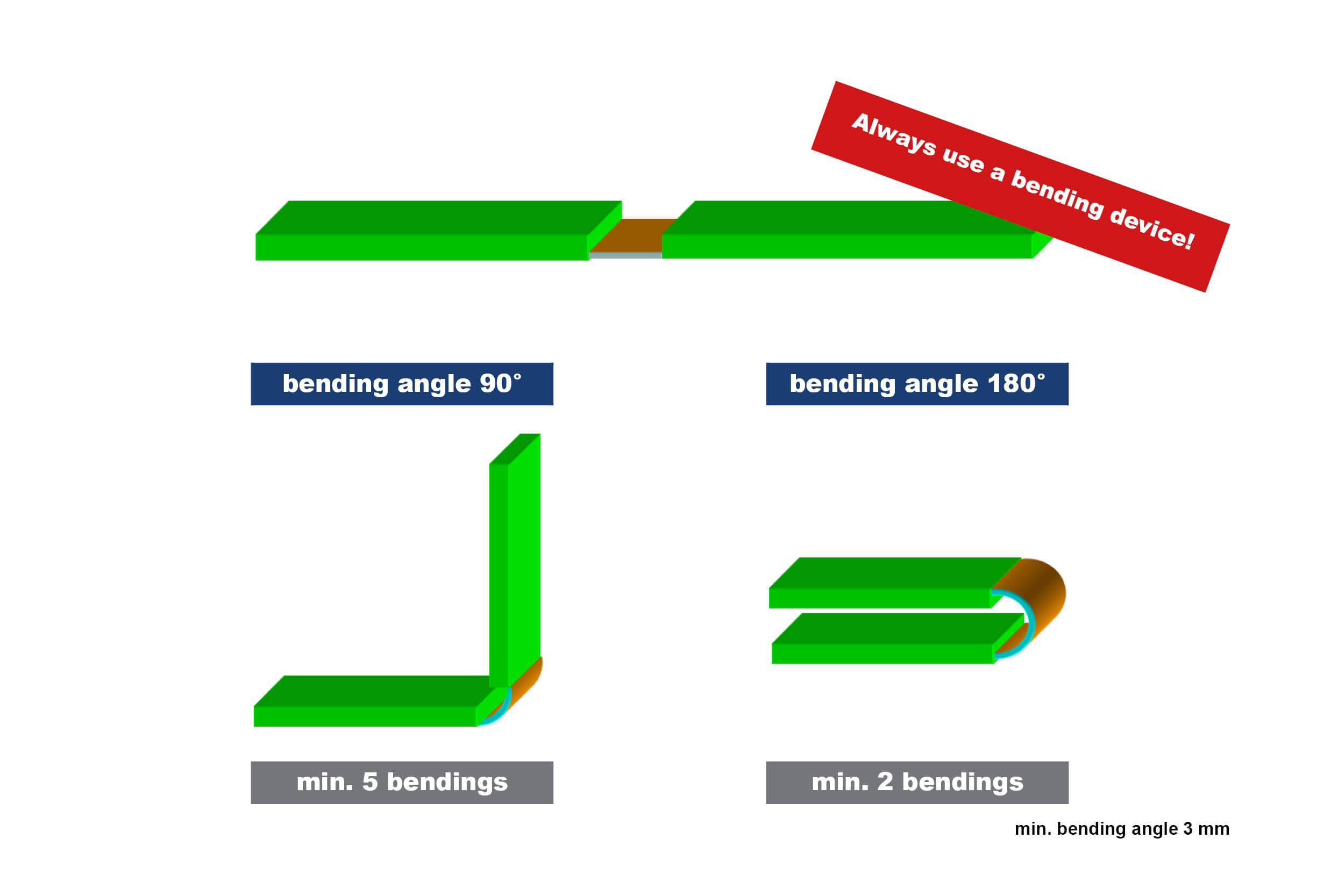
Test printed circuit board - guaranteed bending cycles with different bending angles
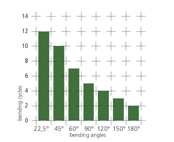
Bending cycles depending on bending angles (min. radius 3 mm)
Specific attention should be paid to the layer structure - especially for designs with two copper layers in the flexible area. Here in particular the require- ments regarding bending radius, bending angle (e.g. 90° or 180°) and the number of bending cycles must be strictly defined. Accordingly, the material (e.g. lead-free soldering) and the struc- tural design must be determined in close coordination with the customer.
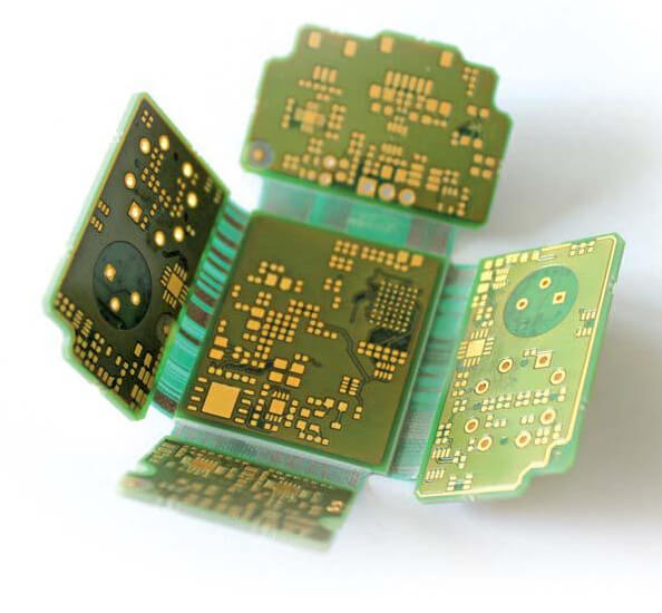
The flexible area can be manufactured in both x-direction and in y-direction
The requirements for the various fields of application differ clearly from each other. That is why Unimicron offers its customers competent technical advice already at an early engineering and project stage in order to translate the specific requirements made of the overall system performance into practice optimally.
Contact to product management:
product management
+49 (0) 2831 - 3 94-0
info@unimicron.de
Further PCB Technologies:
Thick Copper Technology - HiCu PCB | Thick Copper Profile Technology - HiCu Profile PCB | HDI Technology - HiDensity PCB | High Frequency Technology - HiFrequency PCB | Metal Inlay Technology - Metal Inlay PCB | IMS & Heatsink Technology - Metal Plate PCB | Partial Thick Copper Technology - Wirelaid®